莊先生
- 【作業範圍】:(請詳述)
- 【交付方式】:
- 【注意事項】:
- VLSI積體電路設計導論作業
- 1.電子電機科系
- 2.修習過積體電路設計導論
- 3.完成指派任務
- 題目為
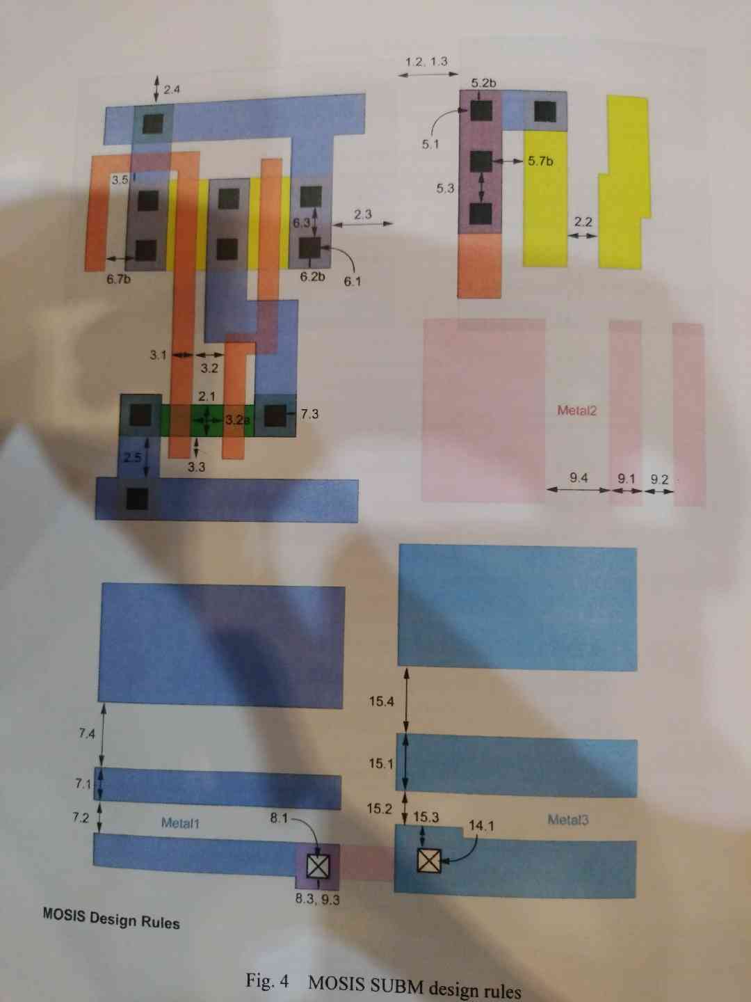
- Q.Consider the schematic of an inverter shown in Fig. 1 and the inverter cross-section in Fig. 2. According to the design rules in Table 1 and Fig. 4, draw the corresponding layout in Fig. 3 for the inverter in an n-well process that has active, p-select, n-select, polysilicon, contact, and metall masks. Include the well contact to VDD and substrate contact to GND.
- Fig. 1 Schematic of an inverter with the aspect ratios (W/L) of 8 λ/2λ and 4 λ/2λ for PMOS and NMOS, respectively
- 請有相關知識在報名
在家兼職
現金、匯款
完成直領
工作日期:2024/10/21~2024/10/28
早班:06:00~08:00
#臨時工 #短期打工
1人
推薦職缺 (20)
-
收購 爭鮮/超商點數
5天前單次$888在家兼職
【幫忙事項】:徵求爭鮮點數3點:1元 【注意事項】: 可轉帳、街口等 另有收購OP點數3點:2元 7-11迪士尼集點6點:1元 7-11安心取件集點1點:2元 全家點數250點:1元 Hami Point 3點:2元 意者請私訊 可以直接告知有什麼點數以及多少點 並告知我需要的付款方式唷,謝謝~
-
(電繪)繪製單曲封面
6天前單次$500在家兼職
【處理事項】:我有寫了一首LO-FI歌曲,想要為這首歌畫一個唱片封面,自己想發Instagram、youtube用的,需要請你用電繪畫,可以的話會動更好 【交付方式】:編輯檔和PNG 【交付期限】:可討論,不急 【注意事項】:請不要有侵犯他人著作財產權的問題
-
徵迪士尼遊行或煙火影片
4天前單次$50在家兼職
【作業範圍】:徵迪士尼遊行或是煙火影片 【交付方式】: email 【注意事項】:長片佳,先傳影片截圖讓我確認畫面品質~謝謝!
-
徵求論壇帳號
1天前單次$30在家兼職
【幫忙事項】: Threads指定文章回覆+按愛心 1.按照方向回覆,字數不限/一則30元 2.會視情況提供圖片 【注意事項】: 1. 留言永久不得刪除 2. 名額結束至關閉前 3.工作時間忙碌不一定會立即回覆 4.每人限定一次
-
❗️❗️🌟店家Google五星評論幫手🌟❗️❗️
1小時前單次$30在家兼職
【評論/分享平台】:❤️❤️Google店家評論❤️❤️ 【分享內容】: 手機行、美髮店、餐廳 等等各類店家都有 ❗️❗️❗️有眾多店家等你評論呦❗️❗️❗️ 👍內容自行發揮字數10-15字左右 👍有時候會有文案(複製貼上即可) 🌟一則5-10元 文字多的10元 或有照片的也是10元 有10的會額外通知(每個任務皆不同哦) 🌟如有多個帳號者佳 會依照帳號健康的持續給案🌟 想要額外多增加收入嗎❓只要簡單評論就能賺錢呦! 【注意事項】: 評論完 無痕模式未登入確認有看到帳號才算成功 支付方式:國泰、中信、台新、ipass
-
剪短影片
1天前單次$500在家兼職
【處理事項】:將課程已錄製好的素材剪輯成指定風格的一支短影片,會提供素材檔案、過往作品的參考影片,影片一支計算 500 元 【交付方式】:上傳 Google drive 的雲端檔案 【交付期限】:雙方討論後再決定 【注意事項】:有作品集的優先,沒有作品也歡迎但是要說明為什麼值得和你合作 請直接按應徵!問問題不要問找到人了沒! 只要任務尚未關閉就是還沒有找到人 備註: - 非華南銀行帳戶將扣 30 元手續費 - 本月底簽領勞保單 - 隔月 10 號匯款薪資
-
代訂徐家私廚🍽️
1天前單次$500在家兼職
幫忙事項】:代訂徐家私廚 久聞徐家私廚美味但卻無法其門而入。希望有熟客能協助代訂位🍽️ 好朋友生日非常想吃,希望能給她一個驚喜❤️
-
徵增肌減脂專家
2天前單次$500在家兼職
徵增肌減脂專家,有相關背景或是經驗者佳,希望能分享增肌減脂的具體方式,主要是針對腹部跟臀部脂肪,確認報價後才開始進行,酬勞可議
-
五星評論
3天前單次$30在家兼職
【評論/分享平台】:五星評論 【任務描述】: 1.五星評論永久不得刪除、更改 2.需保密商家資訊 3.一則評論$5-15元,一個帳號限留一次 4.評論完需用【無痕模式】截圖給我,確認無誤會支薪 5.直接應徵即可 6.使用ipass money、台新支付
-
照明軟體計算
6天前單次$1500在家兼職
【幫忙事項】:(請詳述) 【注意事項】: 會提供燈具配置CAD,需套入DIALUX做計算,出一份簡報資料
-
🍄徵評論小幫手
10小時前單次$30在家兼職
於Google地圖寫評論 🔆有文案,1則10元,一則10元 💰可ipass或郵局帳戶 其他銀行帳戶累計三則可免手續費 ‼️確認上評後24小時內結帳 人數眾多請耐心等候~ ❌️中途消失半小時和一直已讀,直接封鎖哦
-
收購hami點數
1天前單次$30在家兼職
【幫忙事項】:收購hami點數,2點可換1元 【注意事項】:先轉點後匯款,謝謝
-
google評論 手機即可工作 遠端
2天前單次$100在家兼職
【評論/分享平台】:google評論 【分享內容】: 各類店家都有 內容自行發揮字數15-30字、有時候會有文案or圖片 ❗️一個帳戶一天一則千萬不要僥倖多評 不然帳戶會被標註為異常帳戶❗️ 一則10元/滿10則即可領薪 ❗️一個帳號一天寫一則即可❗️ 🌟多個帳號者佳🌟多個帳號者佳🌟 【交付方式】: 完成後點擊您的評論下方分享網址回報 確認成功後公司會於7~14天(不含假日)撥款 【注意事項】: ❗️請勿同時接其他的評論任務❗️若有同時接其他派單評論建議不要再接❗️ 評論完 無痕模式未登入確認有看到帳號才算成功 失敗需重新評論及回報 支付方式:台企 ❗️跨行需支付手續費❗️
-
徵益生菌專家
5天前單次$300在家兼職
因為市面上品牌眾多,許多吃了也不一定有效,因此徵益生菌專家,拒絕推銷,確認後再進行討論 有使用過益生菌、知道內幕者或是生技醫藥相關背景者提供解答與建議,目標是改善體質改善腸道環境,酬勞可討論
-
word文書處理
1天前單次$200在家兼職
【處理事項】:(請詳述) 【交付方式】: 匯款 【交付期限】: 【注意事項】:非常簡單的文書處理,熟悉word應該半小時內就能完成。
-
拍攝影片
4天前單次$1000在家兼職
【處理事項】:拍攝剪輯3C產品影片一部 【交付方式】:審核可以後放到我們公司網站 【交付期限】: 【注意事項】:蝦皮需要1分鐘內影片
-
google評論(遠距,人須在新竹,限一個帳號)
2天前單次$40在家兼職
【幫忙事項】:於google地圖點新增五顆星,並評論 增加10字以上自由發揮內容或是提供內容貼上,須在新竹 【注意事項】: 人須在新竹 1. Google評論不可刪除,保密商家資訊 2. 文章永久不得刪除 3. 需用無痕模式確認上評發截圖,確認結案完成 4.若評論被屏蔽或無顯示皆不符合該任務。 5.匯款可使用任何一家銀行郵局
-
google評論
1小時前單次$30在家兼職
至指定店家google map評論20字左右好評即可 一則評論10元 最多3則 建議不要頻繁頻論(3天內評論2次以上)
-
應徵Dcard 女孩版發文帳號
1週前單次$30在家兼職
應徵Dcard 女孩版發文帳號 長篇圖文發文 需搭配我方提供商品 自行撰文 (300~500字) 🅥商品為我方寄送、我方負擔運費 🅥發文者帳號身份須為女生 🅥需要發文時間: 10/11~10/30之間不等 🅥私訊通知時會告知哪一天需要發文 「請記得應徵時先提供Dcard帳號的截圖 我們需要活躍發文者」 「如只發過個位數文章、平常沒在用帳號的 請勿應徵」 相關資訊會再私訊通知,麻煩週一至週五請注意訊息回覆 支付報酬方式: 特定IP盲袋*1包+30元 (也就是我方提供撰文的商品)/ 有興趣者可以私訊詢問是哪個IP
-
Google地圖🗺️五星評論 當日匯款(若關閉是在更新,仍可留言)
9小時前單次$30在家兼職
‼️『一則10元』,先應徵 開始工作會詢問 收到回應才會發店家‼️ 🔹時間🔹每天早上9點半左右開始,發完為止 🔹價格🔹 有上評『一則10元』,當日付款 🔹轉帳🔹郵局、任何銀行、街口轉帳 🔹工作🔹於google地圖點按五顆星,會給文案。 🔹數量🔹沒限制,沒屏蔽就能繼續接,依照人數分配決定數量。 注意事項 🔹Google評論不可刪除,保密商家資訊 🔹每天早上9:30左右,有空可以來密我拿工作,依照順序發完為止 🔖屏蔽(沒有上評): 別人(也就是店家的顧客們)看不見你的評論。 🔖確認方式: 用其他帳號下去查看最新評論,出現就是成功。